
























First reported by EE Times Asia
Breakthrough Packaging Enhances Power Density in AOS’s Latest MOSFETs
Stacked-die half-bridge boosts MOSFET power density
From the article
Using a vertically stacked-die design, AOS's DFN6×5 AmpStack package integrates two MOSFETs configured as a high-side/low-side half-bridge. The post Stacked-die half-bridge boosts MOSFET power density appeared first on EDN .
Continue reading on EDNYou might also wanna read
AOS’s 80V power conversion MOSFET features DFN6x5 AmpStack packaging
Electronics Weekly·12h ago
Breakthrough Packaging Enhances Power Density in AOS’s Latest MOSFETs
EE Times Asia·19h ago

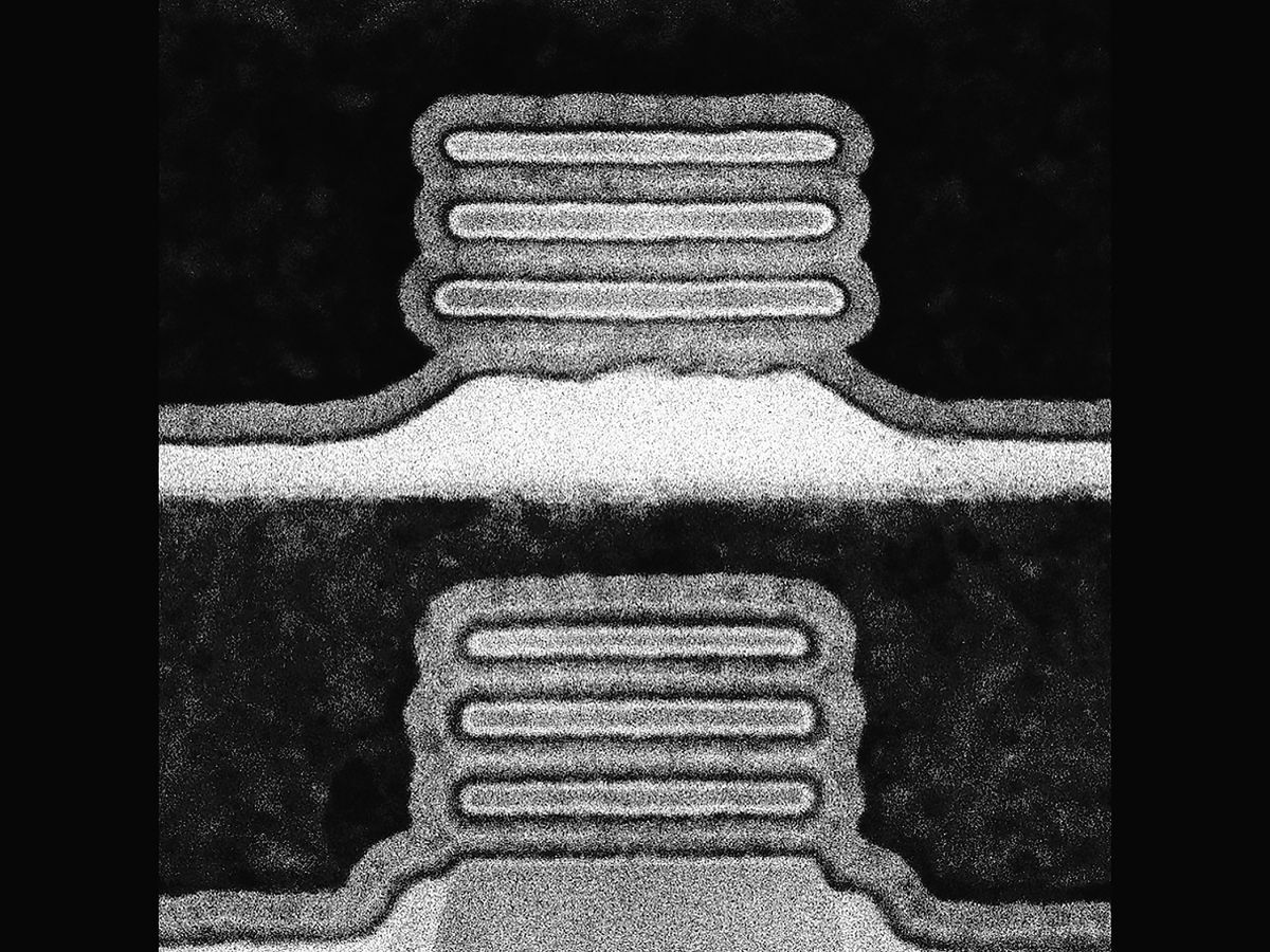
IBM pursues sequential transistor stacking for next-generation chip design, diverging from rivals
IBM has presented research at the IEEE VLSI Symposium detailing a different approach to next-generation transistor design. While all major c
 spectrum.ieee.org·13d ago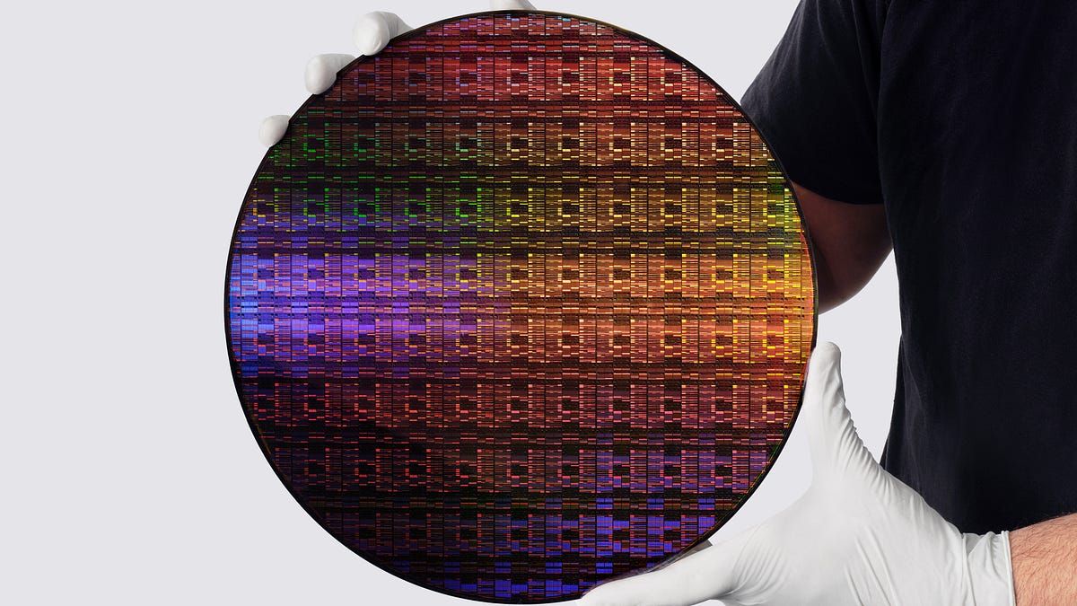
IBM's 0.7nm Node and NanoStack: A Technical Deep Dive into Next-Generation Semiconductor Technology
IBM announces a 0.7nm process node featuring a new transistor architecture called "NanoStack." The article is a deep-dive technical analysis
 morethanmoore.substack.com·13d ago
IBM Unveils 0.7nm Chip Prototype With 100 Billion Transistors Using Novel 3D Nanostack Architecture
IBM has announced the world's first sub-1 nanometer chip technology at the 0.7 nm node, featuring a novel 3D transistor architecture called
 news.bitcoin.com·11d ago
University of Illinois researchers develop 3D chip stacking technique to extend Moore's Law
Researchers at the University of Illinois Grainger College of Engineering have developed a breakthrough in 3D chip manufacturing that could
sciencedaily.com·1mo ago
Comments
Sign in to join the conversation.
No comments yet. Be the first.