
























First reported by EE Times Asia
Breakthrough Packaging Enhances Power Density in AOS’s Latest MOSFETs
AOS’s 80V power conversion MOSFET features DFN6x5 AmpStack packaging
By
Alun Williams
7h agoen
Source
Electronics WeeklyAOS’s 80V power conversion MOSFET features DFN6x5 AmpStack packagingelectronicsweekly.comAlpha and Omega Semiconductor (AOS) is releasing its AOPL66801 80V MOSFET. It is in a half-bridge configuration available in a DFN6x5 AmpStack MOSFET package. The company highlights the packaging technology ... The post AOS’s 80V power conversion MOSFET features DFN6x5 AmpStack packaging appeared first on Electronics Weekly .
You might also wanna read
Breakthrough Packaging Enhances Power Density in AOS’s Latest MOSFETs
EE Times Asia·14h ago
GIGABYTE Puts a True-Color Display Inside a High-Wattage PSU, Case with Display Spanning the Entire Side Panel
techpowerup.com·1mo ago


Data Centers Transition to 800V DC Power Systems for AI Infrastructure Efficiency
The article discusses how data centers are shifting from traditional AC power distribution to 800V DC power systems to meet the increasing e
 spectrum.ieee.org·3mo ago
Analog Devices Completes Acquisition of Empower Semiconductor
EE Times Asia·8h ago
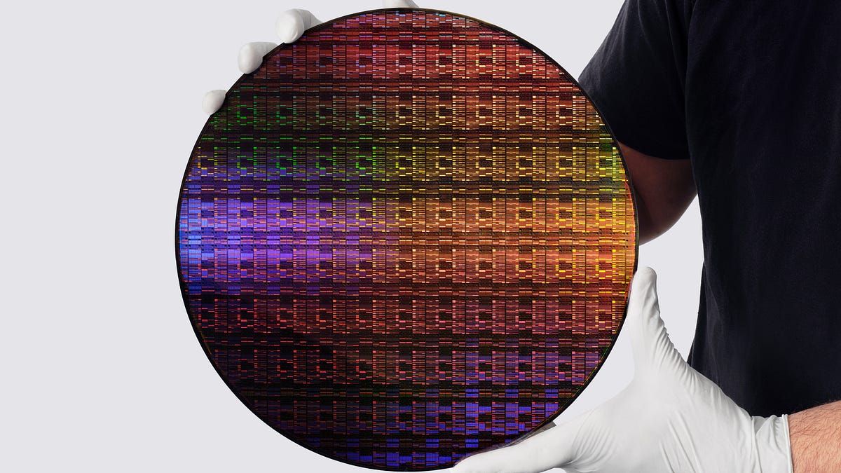
IBM's 0.7nm Node and NanoStack: A Technical Deep Dive into Next-Generation Semiconductor Technology
IBM announces a 0.7nm process node featuring a new transistor architecture called "NanoStack." The article is a deep-dive technical analysis
 morethanmoore.substack.com·13d ago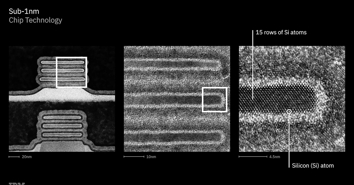
IBM announces 0.7 nm node prototype chips using nanostack transistors
A brief roundup of science and technology news items, including IBM's announcement of prototype chips for the 0.7 nm node using nanostack ga
 nanoscale.blogspot.com·11d ago
Comments
Sign in to join the conversation.
No comments yet. Be the first.