IBM's 0.7nm Node and NanoStack: A Technical Deep Dive into Next-Generation Semiconductor Technology
By
Dr. Ian Cutress
Summary
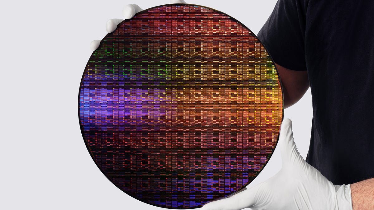
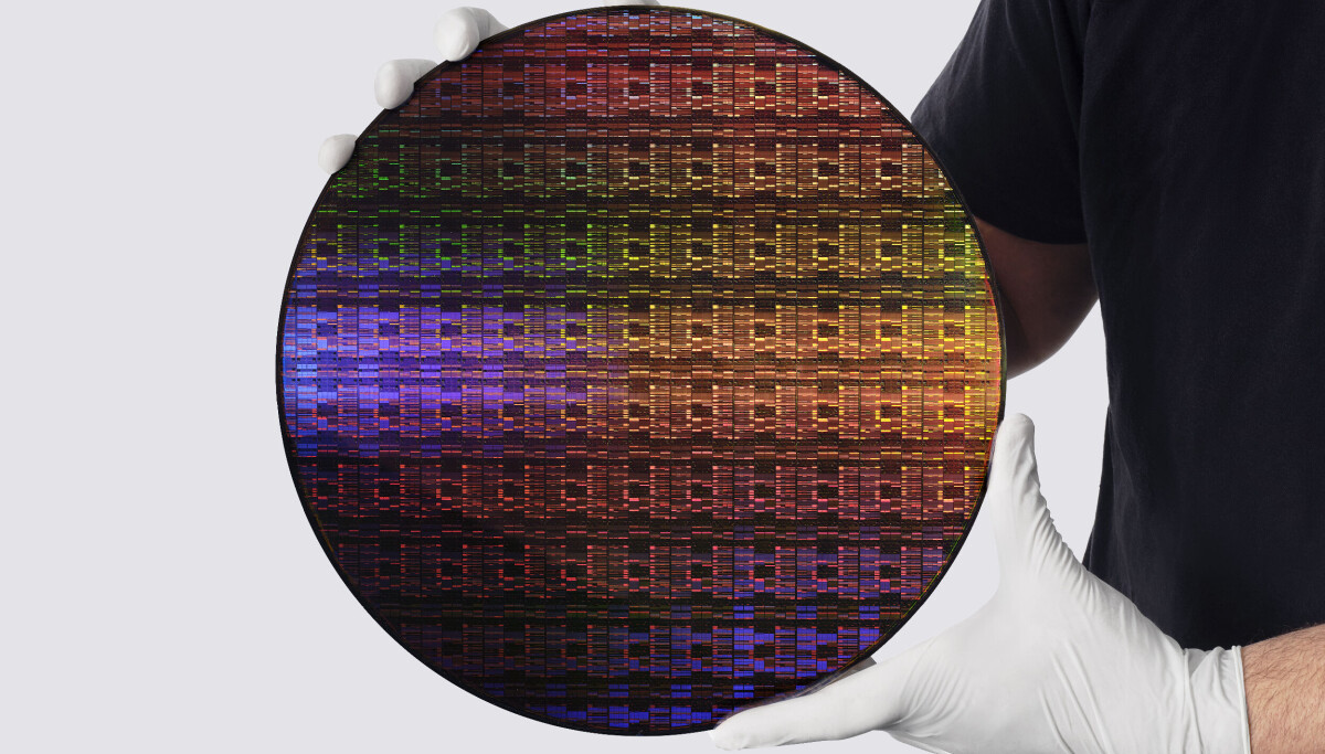
IBM announces a 0.7nm process node featuring a new transistor architecture called "NanoStack." The article is a deep-dive technical analysis from More Than Moore, exploring the implications of this breakthrough for the semiconductor industry, including transistor density of 666 million transistors per square millimeter, the use of High-NA EUV lithography at Albany NanoTech, and the competitive landscape against TSMC, Samsung, and Intel.
Source
 Twitter / XIBM's 0.7nm Node and NanoStack: A Technical Deep Dive into Next-Generation Semiconductor Technologymorethanmoore.substack.com
Key quotes
· 3 pulledThere's a reason why I keep asking high-profile executives and architects at major semiconductor companies about this — the answers reveal where the industry is truly heading.
IBM is going to be using the High-NA EUV machine at Albany NanoTech, not buying their own.
At 666 million transistors per square millimeter, this represents a generational leap in density that challenges conventional scaling roadmaps.
You might also wanna read


IBM Unveils 0.7nm Chip Prototype With 100 Billion Transistors Using Novel 3D Nanostack Architecture
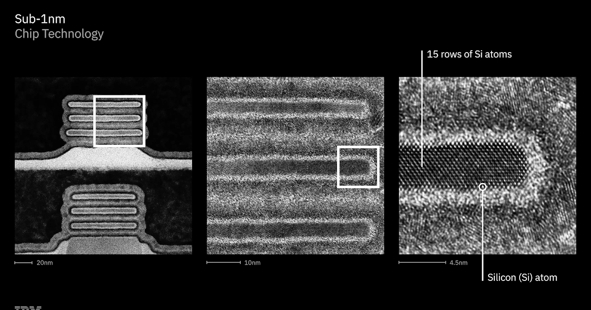
IBM has announced the world's first sub-1 nanometer chip technology at the 0.7 nm node, featuring a novel 3D transistor architecture called
IBM announces 0.7 nm node prototype chips using nanostack transistors
A brief roundup of science and technology news items, including IBM's announcement of prototype chips for the 0.7 nm node using nanostack ga
 nanoscale.blogspot.com·2d ago
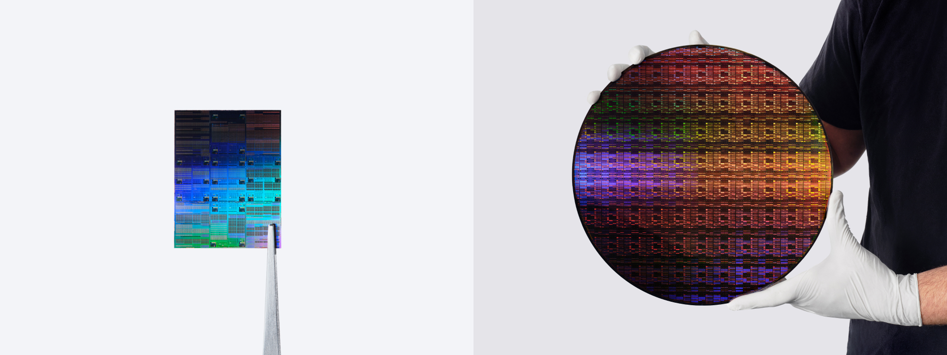
IBM Announces World's First Sub-1 Nanometer Chip with 0.7nm Transistor Architecture
IBM has announced the world's first sub-1 nanometer chip technology, featuring a revolutionary transistor architecture at the 0.7 nm (7 angs
 newsroom.ibm.com·1d ago
IBM Announces World's First Sub-1 Nanometer Chip with 0.7nm Transistor Architecture
IBM has announced the world's first sub-1 nanometer chip technology, featuring a revolutionary transistor architecture at the 0.7 nm (7 angs
newsroom.ibm.com·1d ago
IBM unveils 0.7-nanometer chip with nearly 100 billion transistors, doubling density of 2nm design
IBM has announced the world's first sub-1 nanometer chip with a 0.7nm (7 angstrom) design, integrating nearly 100 billion transistors in a f
IBM announces 0.7 nm chip technology, maps path to 0.1 nm within five years
IBM has announced a sub-nanometer chip technology at the 0.7 nm (7 Angstrom) node, claiming it can cram nearly 100 billion transistors onto
 theregister.com·2d ago
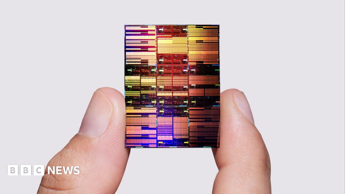
IBM unveils sub-1nm chip design breakthrough, but production still years away
IBM has unveiled a new chip design breakthrough that could enable manufacturers to cram 100 billion transistors onto a silicon chip the size
Comments
Sign in to join the conversation.
No comments yet. Be the first.