IBM Unveils 0.7nm Chip Prototype With 100 Billion Transistors Using Novel 3D Nanostack Architecture
By
Jamie Redman
Summary
IBM has announced the world's first sub-1 nanometer chip technology at the 0.7 nm node, featuring a novel 3D transistor architecture called "nanostack" that stacks transistors vertically in two bonded layers. The prototype packs nearly 100 billion transistors onto a fingernail-sized chip and promises 70% better energy efficiency, extending Moore's Law beyond current silicon limits.
Source

Key quotes
· 3 pulledIBM on Thursday unveiled the world's first sub-1 nanometer chip technology, a research prototype at the 0.7 nanometer node that packs nearly 100 billion transistors onto a chip the size of a fingernail.
The announcement centers on what IBM calls the 'nanostack,' an entirely new three-dimensional transistor architecture developed at its semiconductor research facility in Albany, New York.
The design stacks and staggers transistors vertically in two bonded layers, using an ultra-thin dielectric material to separate them.
You might also wanna read


IBM unveils world's first sub-1 nanometer chip with 0.7nm transistor architecture
IBM has announced the world's first sub-1 nanometer chip technology, featuring a revolutionary transistor architecture at the 0.7 nm (7 angs
 ibm.co·1d ago
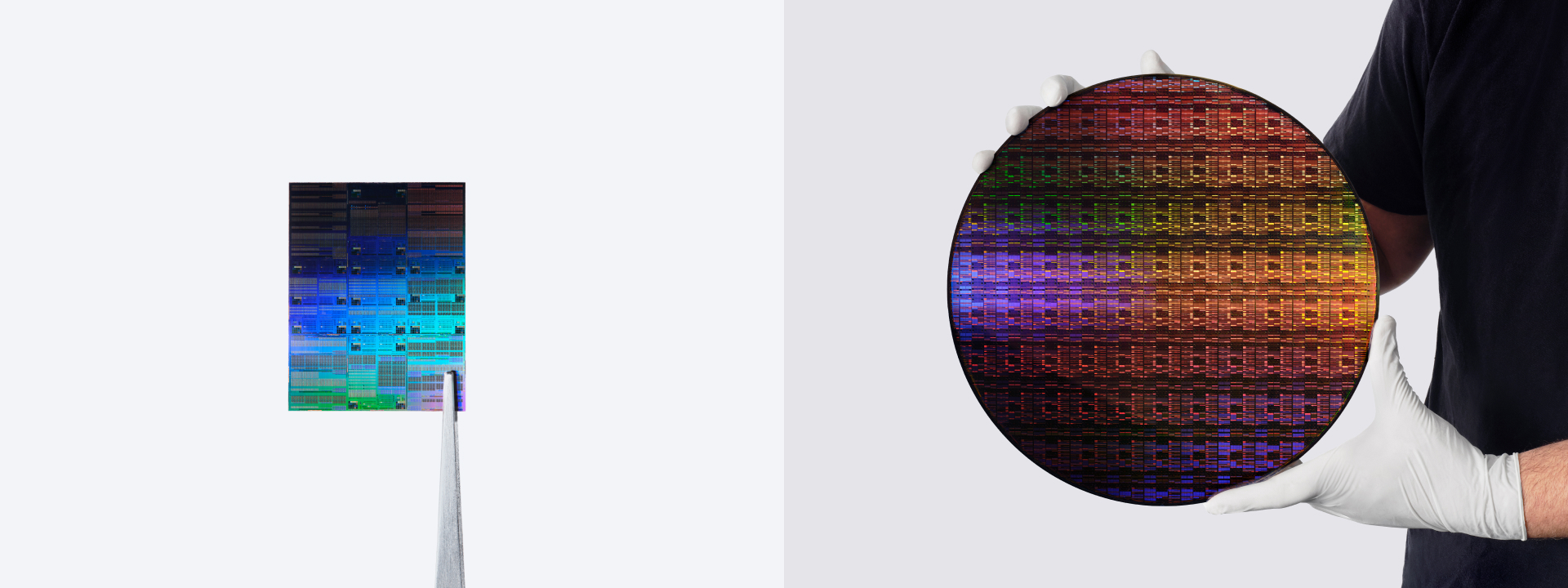
IBM Announces World's First Sub-1 Nanometer Chip with 0.7nm Transistor Architecture
IBM has announced the world's first sub-1 nanometer chip technology, featuring a revolutionary transistor architecture at the 0.7 nm (7 angs
 newsroom.ibm.com·58m ago
IBM Announces World's First Sub-1 Nanometer Chip with 0.7nm Transistor Architecture
IBM has announced the world's first sub-1 nanometer chip technology, featuring a revolutionary transistor architecture at the 0.7 nm (7 angs
newsroom.ibm.com·58m ago
IBM's 3D chip prototype packs 100 billion transistors, doubling current density
IBM has announced a prototype chip that packs nearly 100 billion transistors onto a fingernail-sized 10mm x 15mm chip, nearly doubling the t
 newscientist.com·18h ago
Designing a Systolic Array AI Accelerator in Two Weeks for Global Foundries 180nm Tapeout
The article details the author's ambitious project to design a systolic array AI accelerator with in-silicon debug infrastructure from scrat
 essenceia.github.io·5mo ago
Chinese Researchers Develop Analog Chip Claimed to Be 1,000 Times Faster Than Nvidia GPUs for Specific Applications
Chinese researchers from Peking University have developed a new analog chip using resistive random-access memory (RRAM) technology that repo
 livescience.com·7mo ago
Managing 50 Million Pins: Automated Design Solutions for 3D IC and Chiplet Technology
The article discusses the semiconductor industry's shift to 3D IC technology and chiplets, highlighting the challenges of managing massive p
 allaboutcircuits.com·3mo ago
Comments
Sign in to join the conversation.
No comments yet. Be the first.