IBM's 3D chip prototype packs 100 billion transistors, doubling current density
By
Matthew Sparkes
Summary
IBM has announced a prototype chip that packs nearly 100 billion transistors onto a fingernail-sized 10mm x 15mm chip, nearly doubling the transistor count of the previous state-of-the-art. This breakthrough is achieved through a three-dimensional technique that adds a second layer of silicon circuitry. The chip promises 70% higher energy efficiency and 50% higher performance compared to current leading chips, though commercial availability is still 5-10 years away.
Source

 Twitter / XIBM's 3D chip prototype packs 100 billion transistors, doubling current densitynewscientist.com
Key quotes
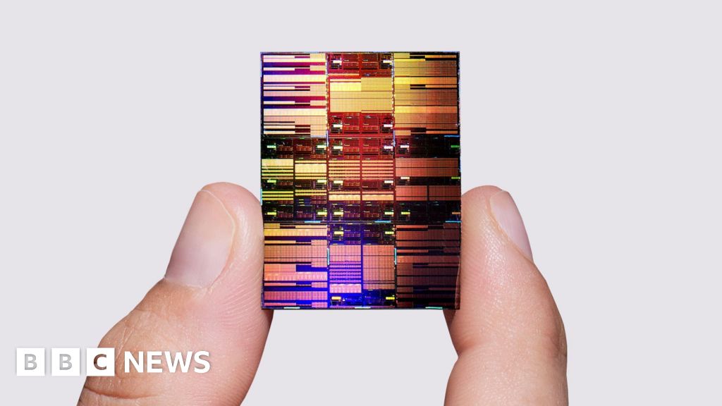
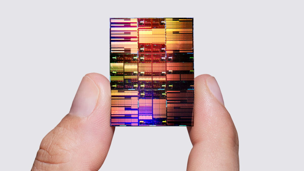
· 2 pulledIBM's prototype chip is the size of a fingernail, yet packs in almost 100 billion transistors – nearly twice as many as the previous state-of-the-art chip – thanks to a three-dimensional technique.
The company says the 10 millimetre by 15 millimetre chip will offer 70 per cent higher energy efficiency and 50 per cent higher performance than current leading chips, and will be in commercial devices within 10 years.
You might also wanna read

IBM unveils sub-1 nanometre chip design, packing 100 billion transistors on a fingernail-sized surface
IBM has unveiled a new chip design breakthrough below 1 nanometre, enabling up to 100 billion transistors to be packed onto a chip the size
 bbc.com·1d ago
IBM Unveils 0.7nm Chip Prototype With 100 Billion Transistors Using Novel 3D Nanostack Architecture
IBM has announced the world's first sub-1 nanometer chip technology at the 0.7 nm node, featuring a novel 3D transistor architecture called

IBM unveils 0.7-nanometer chip with nearly 100 billion transistors, doubling density of 2nm design
IBM has announced the world's first sub-1 nanometer chip with a 0.7nm (7 angstrom) design, integrating nearly 100 billion transistors in a f
IBM announces world's first sub-1 nanometer chip, packing 100 billion transistors
IBM has announced a breakthrough in semiconductor technology with the world's first sub-1 nanometer chip. The chip packs nearly 100 billion
 gizmodo.com·1d ago
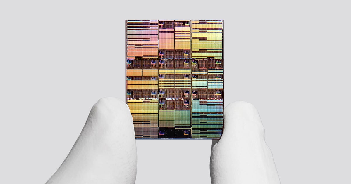
IBM announces sub-1 nanometre chip technology with nearly 100 billion transistors
IBM has announced what it claims is the world's first sub-1 nanometre chip technology, packing nearly 100 billion transistors onto a chip th
 thenationalnews.com·19h ago
IBM unveils sub-1nm chip design breakthrough, but production still years away
IBM has unveiled a new chip design breakthrough that could enable manufacturers to cram 100 billion transistors onto a silicon chip the size
Comments
Sign in to join the conversation.
No comments yet. Be the first.