IBM Announces World's First Sub-1 Nanometer Chip with 0.7nm Transistor Architecture
By
porridgeraisin
Summary
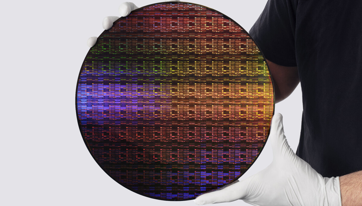
IBM has announced the world's first sub-1 nanometer chip technology, featuring a revolutionary transistor architecture at the 0.7 nm (7 angstrom) node. This breakthrough uses a novel "nanostack" 3D chip architecture that stacks transistors vertically rather than shrinking them horizontally, allowing more transistors per square millimeter. The achievement represents a major milestone for the semiconductor industry, which has been approaching the physical limits of traditional chip scaling. IBM's innovation promises to propel the industry forward for the next decade by enabling more powerful and energy-efficient processors.
Source

 Hacker NewsIBM Announces World's First Sub-1 Nanometer Chip with 0.7nm Transistor Architecturenewsroom.ibm.com
Key quotes
· 3 pulledIBM today unveiled a major semiconductor breakthrough with the introduction of the world's first sub-1 nanometer (nm) chip technology, featuring a revolutionary transistor architecture at the 0.7 nm, or 7 angstrom node.
The achievement marks a landmark moment for an industry facing the physical limits of traditional chip scaling.
Built with revolutionary 'nanostack' 3D chip architecture, IBM's sub-1 nm chip to propel semiconductor industry forward for the next decade
You might also wanna read


IBM unveils world's first sub-1 nanometer chip with 0.7nm transistor architecture
IBM has announced the world's first sub-1 nanometer chip technology, featuring a revolutionary transistor architecture at the 0.7 nm (7 angs
 ibm.co·14h ago
IBM announces world's first sub-1 nanometer chip, packing 100 billion transistors
IBM has announced a breakthrough in semiconductor technology with the world's first sub-1 nanometer chip. The chip packs nearly 100 billion
 gizmodo.com·10h ago
IBM unveils sub-1nm chip design breakthrough, but production still years away
IBM has unveiled a new chip design breakthrough that could enable manufacturers to cram 100 billion transistors onto a silicon chip the size
IBM announces 0.7 nm chip technology, maps path to 0.1 nm within five years
IBM has announced a sub-nanometer chip technology at the 0.7 nm (7 Angstrom) node, claiming it can cram nearly 100 billion transistors onto
 theregister.com·3h ago
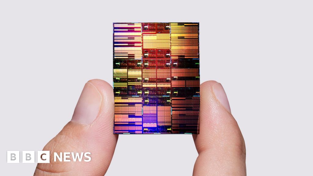
IBM unveils sub-1 nanometre chip design, packing 100 billion transistors on a fingernail-sized surface
IBM has unveiled a new chip design breakthrough below 1 nanometre, enabling up to 100 billion transistors to be packed onto a chip the size
 bbc.com·19h ago
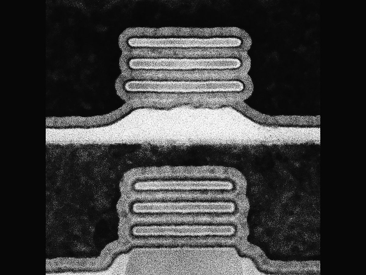
IBM pursues sequential transistor stacking for next-generation chip design, diverging from rivals
IBM has presented research at the IEEE VLSI Symposium detailing a different approach to next-generation transistor design. While all major c
 spectrum.ieee.org·1d ago
Comments
Sign in to join the conversation.
No comments yet. Be the first.