IBM pursues sequential transistor stacking for next-generation chip design, diverging from rivals
By
Samuel K. Moore
Summary
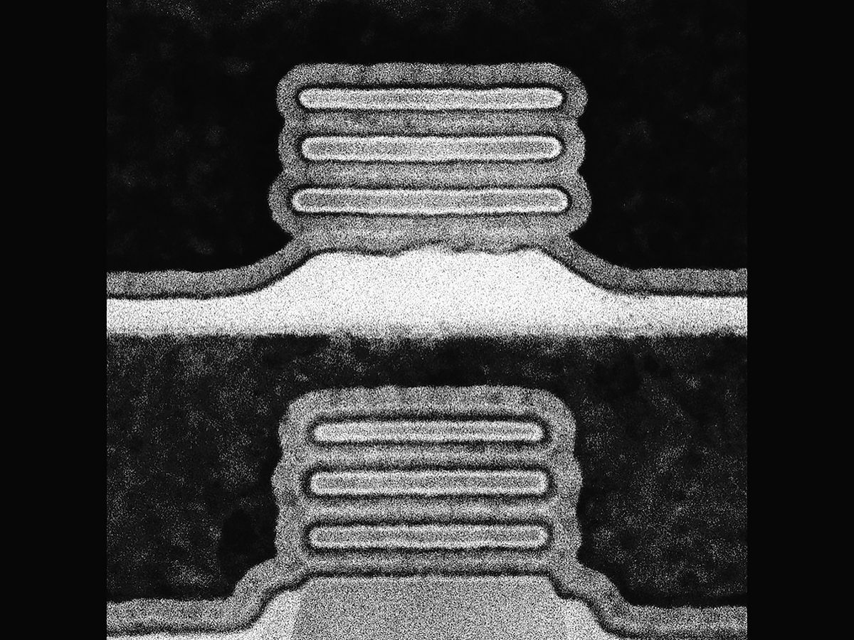
IBM has presented research at the IEEE VLSI Symposium detailing a different approach to next-generation transistor design. While all major chipmakers agree that future transistors will involve stacking two transistors vertically (complementary FET or CFET), IBM's path diverges from Intel, Samsung, and TSMC. IBM is pursuing a sequential stacking approach where the bottom transistor is built first, then the top transistor is fabricated on top using lower-temperature processes. This contrasts with the monolithic approach favored by others, where both transistors are built simultaneously. The sequential method offers advantages in design flexibility and thermal budget management but introduces challenges in alignment and defect control. Commercial introduction is expected around 2030.
Source
 bskyIBM pursues sequential transistor stacking for next-generation chip design, diverging from rivalsspectrum.ieee.org
Key quotes
· 3 pulledChipmakers agree that the transistor of the next decade will actually be two transistors stacked atop one another, packing in many more devices in the same area of silicon and leading to circuits that are as little as half the size of today's.
But their research efforts are beginning to show some important divergence in the details.
Commercial introduction is likely six years away, so they are far from a final version, but research presented last week at IEEE VLSI Symposium in Honolulu and detailed today by IBM points toward two main paths.
You might also wanna read


Industry Experts Discuss AI Applications in Semiconductor Chip Design
This article features a roundtable discussion with semiconductor industry experts from Cadence, Siemens EDA, Synopsys, Baya Systems, ChipAge
Bridging the Semiconductor Talent Gap: Cross-Training CS Students and AI-Assisted Hardware Design
The article discusses innovative approaches to address the talent shortage in the semiconductor industry, including cross-training computer
Designing a Systolic Array AI Accelerator in Two Weeks for Global Foundries 180nm Tapeout
The article details the author's ambitious project to design a systolic array AI accelerator with in-silicon debug infrastructure from scrat
 essenceia.github.io·5mo ago
Huawei has outlined a new approach to chip design — a departure from the decades-long industry focus on shrinking transistors to improve performance. Here's why it has investors buzzing. https://t.co/
FPGA Based IBM-PC-XT

TSMC CEO says chipmaker is struggling to meet AI-driven demand despite US factory expansion
TSMC, the world's largest semiconductor manufacturer, is struggling to meet surging customer demand driven by the AI boom, even with its ong
Comments
Sign in to join the conversation.
No comments yet. Be the first.