IBM announces 0.7 nm chip technology, maps path to 0.1 nm within five years
By
Dan Robinson
Summary
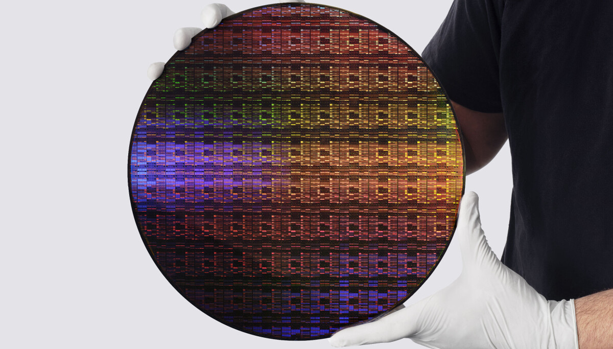
IBM has announced a sub-nanometer chip technology at the 0.7 nm (7 Angstrom) node, claiming it can cram nearly 100 billion transistors onto a fingernail-sized die — almost double the density of its 2021 2 nm technology. The company has mapped a path down to 0.1 nm (1 Angstrom) and says commercial chips using this process could be available within five years. The announcement positions IBM as a leader in advanced semiconductor research, though the technology is still years away from mass production.
Source
 bskyIBM announces 0.7 nm chip technology, maps path to 0.1 nm within five yearstheregister.com
Key quotes
· 3 pulledIBM has developed a sub-nanometer (nm) chip technology it says could be used to produce commercial chips within five years, and has mapped a path to 0.1 nm.
Big Blue claims its new process node can cram nearly 100 billion transistors onto a silicon die the size of a fingernail, almost double the density of the 2 nm technology it unveiled back in 2021.
The new process as disclosed is actually for 0.7 nm or 7 Angstroms (7A), compared with the cutting-edge manufacturing nodes now being prepared for production in 2028.
You might also wanna read


IBM unveils world's first sub-1 nanometer chip with 0.7nm transistor architecture
IBM has announced the world's first sub-1 nanometer chip technology, featuring a revolutionary transistor architecture at the 0.7 nm (7 angs
 ibm.co·12h ago
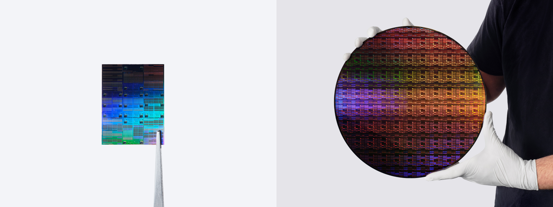
IBM Announces World's First Sub-1 Nanometer Chip with 0.7nm Transistor Architecture
IBM has announced the world's first sub-1 nanometer chip technology, featuring a revolutionary transistor architecture at the 0.7 nm (7 angs
 newsroom.ibm.com·18h ago
Chinese Researchers Develop Analog Chip Claimed to Be 1,000 Times Faster Than Nvidia GPUs for Specific Applications
Chinese researchers from Peking University have developed a new analog chip using resistive random-access memory (RRAM) technology that repo
 livescience.com·7mo ago
IBM Announces Six Technology Roadmaps for Next-Generation Computing
IBM is introducing six technology roadmaps aimed at advancing computing performance and efficiency for information technology and business a
 ibm.com·9mo ago
Designing a Systolic Array AI Accelerator in Two Weeks for Global Foundries 180nm Tapeout
The article details the author's ambitious project to design a systolic array AI accelerator with in-silicon debug infrastructure from scrat
 essenceia.github.io·5mo ago
TSMC to Manufacture Advanced 3-Nanometer AI Chips in Japan
TSMC, the world's largest contract chipmaker, announced it will manufacture advanced 3-nanometer semiconductors in Japan to meet booming AI
 apnews.com·4mo ago
Comments
Sign in to join the conversation.
No comments yet. Be the first.