
























Breakthrough Packaging Enhances Power Density in AOS’s Latest MOSFETs
By
Stephen Las Marias
9h agoen
Source
EE Times AsiaBreakthrough Packaging Enhances Power Density in AOS’s Latest MOSFETseetasia.comAOS's breakthrough packaging technology enables high-density designs for various power conversion applications. The post Breakthrough Packaging Enhances Power Density in AOS’s Latest MOSFETs appeared first on EE Times Asia .
You might also wanna read


Applied Materials VP discusses AI, energy demands, and semiconductor innovation beyond traditional scaling
In this interview, Sundeep Bajikar, VP of Corporate Strategy and Marketing at Applied Materials, discusses how the semiconductor industry is
 euractiv.com·6d ago
Scientists just measured the smallest possible contacts for future computer chips
Phys·1d ago
Nexperia’s 1200 V SiC MOSFETs in QDPAK packaging
Electronics Weekly·21h ago
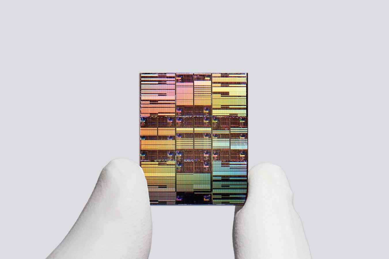
IBM's 3D chip prototype packs 100 billion transistors, doubling current density
IBM has announced a prototype chip that packs nearly 100 billion transistors onto a fingernail-sized 10mm x 15mm chip, nearly doubling the t
 newscientist.com·11d ago
IBM's 3D chip prototype packs 100 billion transistors, doubling current density
IBM has announced a prototype chip that packs nearly 100 billion transistors onto a fingernail-sized 10mm x 15mm chip, nearly doubling the t
newscientist.com·11d ago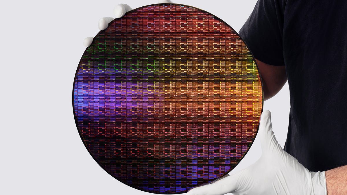
IBM's 0.7nm Node and NanoStack: A Technical Deep Dive into Next-Generation Semiconductor Technology
IBM announces a 0.7nm process node featuring a new transistor architecture called "NanoStack." The article is a deep-dive technical analysis
 morethanmoore.substack.com·13d ago
University of Illinois researchers develop 3D chip stacking technique to extend Moore's Law
Researchers at the University of Illinois Grainger College of Engineering have developed a breakthrough in 3D chip manufacturing that could
sciencedaily.com·1mo ago
Comments
Sign in to join the conversation.
No comments yet. Be the first.