IBM Unveils Sub-1 Nanometer Chip Technology With 0.7nm Transistors
By
eriHwBusters
Summary
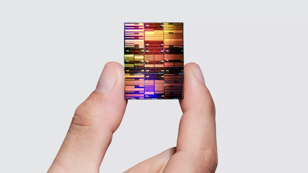
IBM has announced a breakthrough in chip design, unveiling what it calls the world's first sub-1 nanometer node chip technology with transistors measuring just 0.7 nanometers (7 angstroms) wide. This advancement could enable manufacturers to pack 100 billion transistors onto a chip the size of a fingernail, representing a significant leap in semiconductor miniaturization.
Source
Key quotes
· 5 pulledIBM has unveiled a new chip design it calls the world's first sub 1 nanometer node chip technology.
The transistors are just 0.7 nanometers (7 angstroms) wide.
This makes them the smallest transistors in the world by some margin.
The design could enable manufacturers to cram 100 billion transistors on a chip the size of a fingernail.
A human red blood cell is about 7,000 nanometers wide. That is about 10,000 times larger than one of these new nodes.
You might also wanna read


IBM unveils world's first sub-1 nanometer chip with 0.7nm transistor architecture
IBM has announced the world's first sub-1 nanometer chip technology, featuring a revolutionary transistor architecture at the 0.7 nm (7 angs
 ibm.co·9d ago
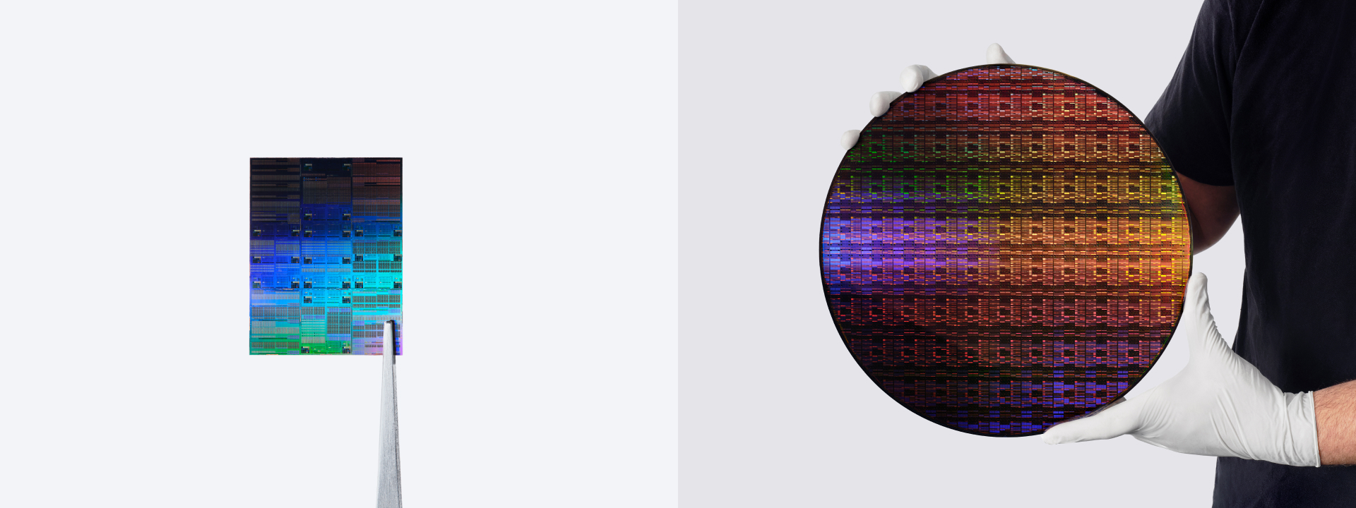
IBM Announces World's First Sub-1 Nanometer Chip with 0.7nm Transistor Architecture
IBM has announced the world's first sub-1 nanometer chip technology, featuring a revolutionary transistor architecture at the 0.7 nm (7 angs
 newsroom.ibm.com·7d ago
IBM Announces World's First Sub-1 Nanometer Chip with 0.7nm Transistor Architecture
IBM has announced the world's first sub-1 nanometer chip technology, featuring a revolutionary transistor architecture at the 0.7 nm (7 angs
newsroom.ibm.com·7d ago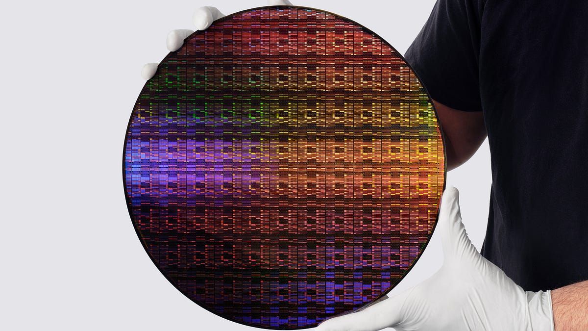
IBM's 0.7nm Node and NanoStack: A Technical Deep Dive into Next-Generation Semiconductor Technology
IBM announces a 0.7nm process node featuring a new transistor architecture called "NanoStack." The article is a deep-dive technical analysis
 morethanmoore.substack.com·9d ago
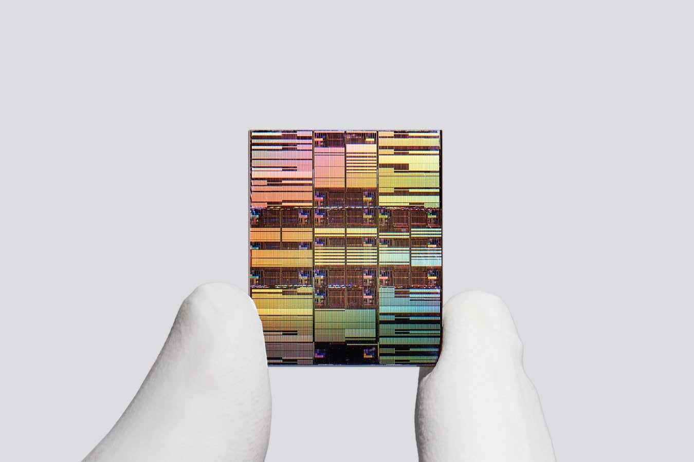
IBM's 3D chip prototype packs 100 billion transistors, doubling current density
IBM has announced a prototype chip that packs nearly 100 billion transistors onto a fingernail-sized 10mm x 15mm chip, nearly doubling the t
 newscientist.com·8d ago
TSMC to Manufacture Advanced 3-Nanometer AI Chips in Japan
TSMC, the world's largest contract chipmaker, announced it will manufacture advanced 3-nanometer semiconductors in Japan to meet booming AI
 apnews.com·4mo ago
Designing a Systolic Array AI Accelerator in Two Weeks for Global Foundries 180nm Tapeout
The article details the author's ambitious project to design a systolic array AI accelerator with in-silicon debug infrastructure from scrat
 essenceia.github.io·5mo ago
Comments
Sign in to join the conversation.
No comments yet. Be the first.