Directly probing the carrier transfer length in 2D-material transistors
By
Ya-Ping Chiu
Source
 Nature CommunicationsDirectly probing the carrier transfer length in 2D-material transistorsnature.com
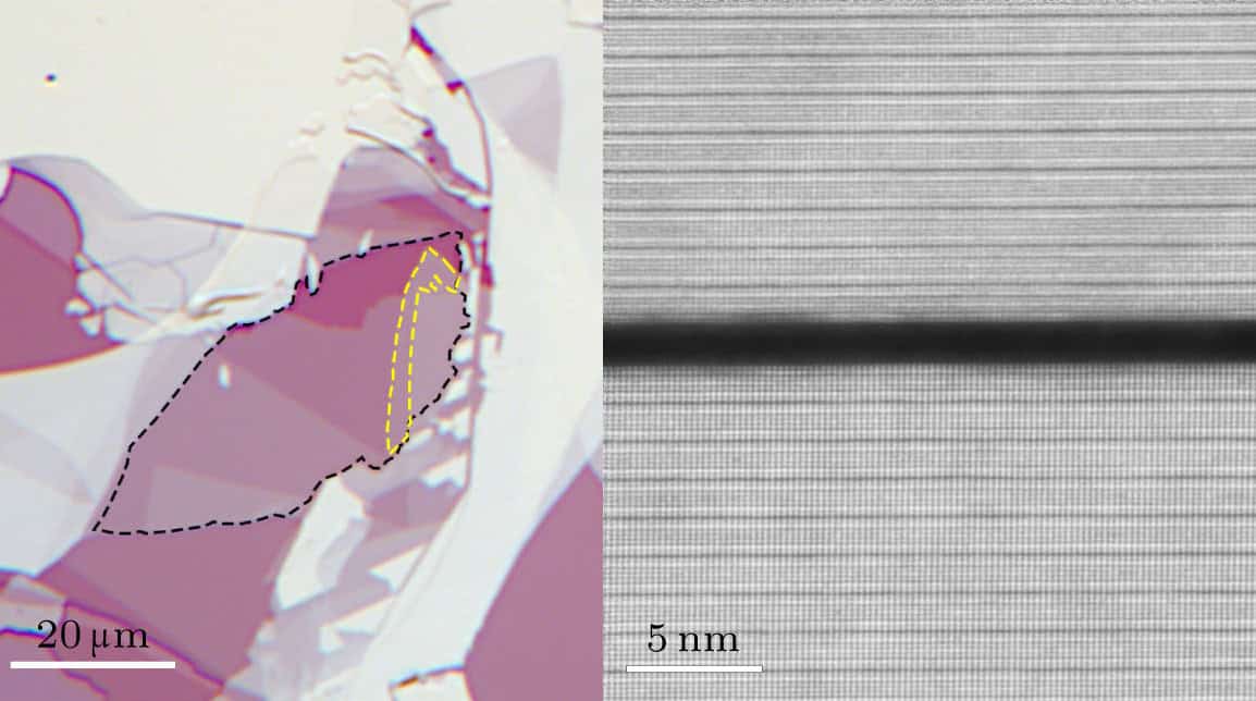
Nature, Published online: 01 July 2026; doi:10.1038/s41586-026-10707-0 Cross-sectional scanning tunnelling microscopy shows a 2 nm carrier transfer length in bismuth-contacted monolayer MoS2 transistors, defining metal-contact scaling limits for sub-10 nm 2D electronic devices.
You might also wanna read
Scaling nanoribbon transistors with monolayer transition metal dichalcogenides
dlvr.it·1mo ago

New encapsulation technique enables first direct imaging of top surface in 2D quantum material
Researchers have developed a new encapsulation technique that allows, for the first time, direct imaging of the top surface structure of ato
physicsworld.com·11d ago

Atomically precise carbon structure fabrication demonstrated using inverted-mode STM mechanosynthesis
Researchers demonstrate atomically precise mechanosynthesis of carbon structures on a hydrogen-passivated Si(100) surface using inverted-mod

Multi-gate ferroelectric transistor based on CuInP2S6/MoS2 heterojunctions integrates digital and analog functions
This article presents a research breakthrough in two-dimensional ferroelectric van der Waals heterojunctions, specifically a multi-gate asym
cell.com·2d ago

Nature research paper: Optical cooling by interfacial charge transfer in 2D heterostructures
go.nature.com
Encapsulation enhances surface structure imaging of 2D quantum material
iop.org·11d ago
Comments
Sign in to join the conversation.
No comments yet. Be the first.