Ultra-high quality factor superconducting tantalum resonators fabricated on 300 mm silicon wafers
By
[Submitted on 9 Jun 2026]
Master baker tier. Every paragraph earns its place on the tray.
Summary
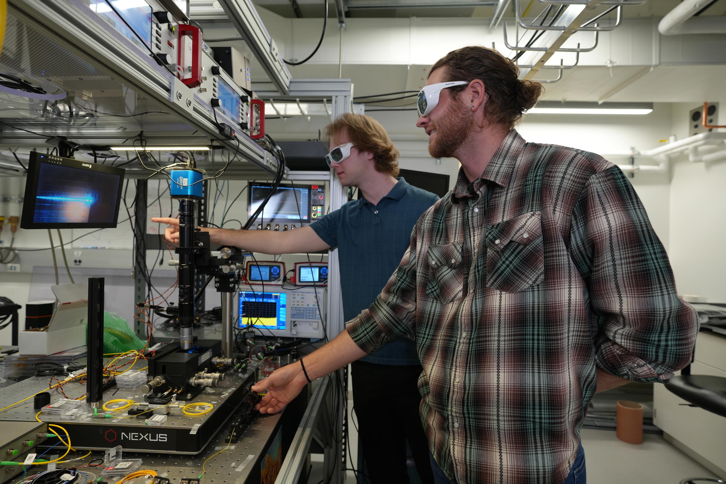
This research paper reports the fabrication of ultra-high quality factor superconducting tantalum (α-Ta) resonators on 300 mm ultra-high-resistivity intrinsic silicon wafers using industrial processes. The resonators achieved median internal quality factors exceeding 40 million and maxima above 60 million. The study identifies a dominant interface loss mechanism and places conservative upper bounds on substrate-associated dissipation, with the best-performing substrate showing a loss tangent below 1.0 × 10⁻⁸. The findings establish industrial 300 mm processing and MCZ silicon as a promising platform for superconducting quantum architectures requiring ultra-high quality factors.
Key quotes
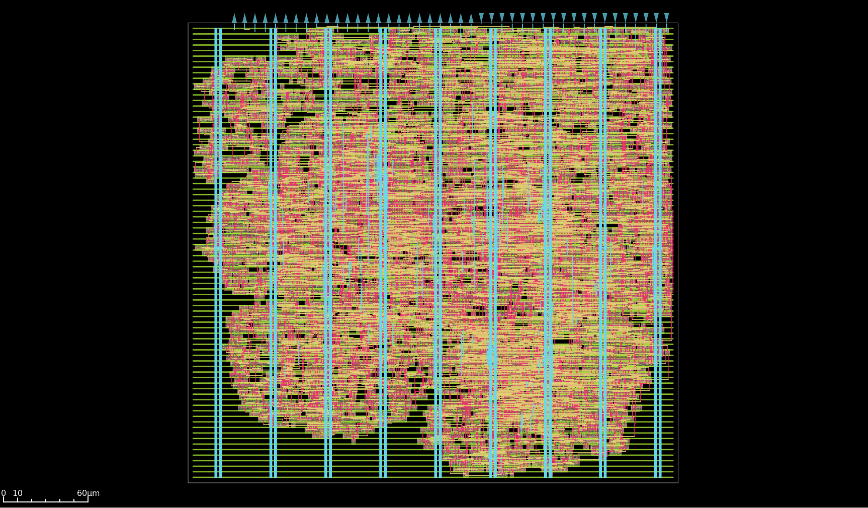
· 3 pulledHere we report planar α-Ta resonators fabricated on 300 mm ultra-high-resistivity (>10 kΩ cm) intrinsic silicon using industrial processes, achieving median internal Q factors exceeding 40 million and maxima above 60 million.
For the best-performing substrate, the inferred substrate loss tangent is below 1.0 × 10⁻⁸, establishing industrial MCZ silicon among the lowest-loss substrate platforms reported for superconducting resonators.
More broadly, these studies establish industrial 300 mm processing, careful interface engineering, and 300 mm MCZ silicon substrates as a promising platform for resonator-heavy superconducting quantum architectures with ultra-high quality factors.
You might also wanna read

NIST Scientists Develop Integrated Photonic Circuits for Tunable Wavelength Lasers
NIST scientists and collaborators have developed a breakthrough method for creating integrated photonic circuits that can generate laser lig
 nist.gov·1mo ago
447 TB/cm² at zero retention energy – atomic-scale memory on fluorographane
Designing a Systolic Array AI Accelerator in Two Weeks for Global Foundries 180nm Tapeout
The article details the author's ambitious project to design a systolic array AI accelerator with in-silicon debug infrastructure from scrat
 essenceia.github.io·4mo ago
Stanford's Diamond Thermal Conductivity Breakthrough for Advanced Chip Cooling
The article discusses the critical challenge of heat management in modern computing as transistors become smaller and more densely packed. I
 spectrum.ieee.org·7mo ago
Atomically precise carbon structure fabrication demonstrated using inverted-mode STM mechanosynthesis
Researchers demonstrate atomically precise mechanosynthesis of carbon structures on a hydrogen-passivated Si(100) surface using inverted-mod

Texas Institute for Electronics Transforms 1980s Fab into World's Only 3D Heterogeneous Integration Facility for DARPA Program
The Texas Institute for Electronics (TIE) in Austin, Texas, is transforming a 1980s-era semiconductor fab into the world's only advanced pac
spectrum.ieee.org·7mo ago