
























IBM announces world's first sub-1-nanometer chip technology using nanostack architecture
IBM was the first in the world to develop a chip architecture with transistors on a scale of less than 1 nanometer.
Read the full articleYou might also wanna read

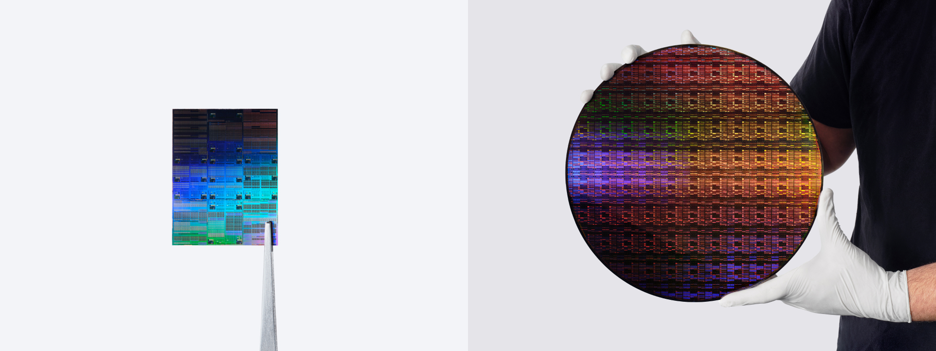
IBM Announces World's First Sub-1 Nanometer Chip with 0.7nm Transistor Architecture
IBM unveiled a major semiconductor breakthrough with the introduction of the world’s first sub-1 nanometer (nm) chip technology, featuring a
 newsroom.ibm.com·20d ago
IBM Announces World's First Sub-1 Nanometer Chip with 0.7nm Transistor Architecture
IBM unveiled a major semiconductor breakthrough with the introduction of the world’s first sub-1 nanometer (nm) chip technology, featuring a
IBM·20d agoIBM Announces World's First Sub-1 Nanometer Chip with 0.7nm Transistor Architecture
IBM unveiled a major semiconductor breakthrough with the introduction of the world’s first sub-1 nanometer (nm) chip technology, featuring a
newsroom.ibm.com·20d ago
IBM unveils world's first sub-1 nanometer chip with 0.7nm transistor architecture
IBM unveiled a major semiconductor breakthrough with the introduction of the world’s first sub-1 nanometer (nm) chip technology, featuring a
 ibm.co·22d ago
IBM: World’s First Sub-1-Nanometer Chip Technology Unveiled
June 25, 2026. On June 25, IBM unveiled a major breakthrough in semiconductor technology: the world’s first sub-1-nanometer (nm) chip techno
IBM introduces the smallest computer chip in the world
It’s the world’s first sub-1nm chip technology, powered by IBM’s new nanostack architecture, paving the way for more powerful chips for year
Look Past IBM’s 0.7nm Label: Nanostack Architecture Is the Real Breakthrough
IBM’s nanostack architecture represents the real breakthrough in chip technology, delivering 50% more performance and 70% greater energy eff
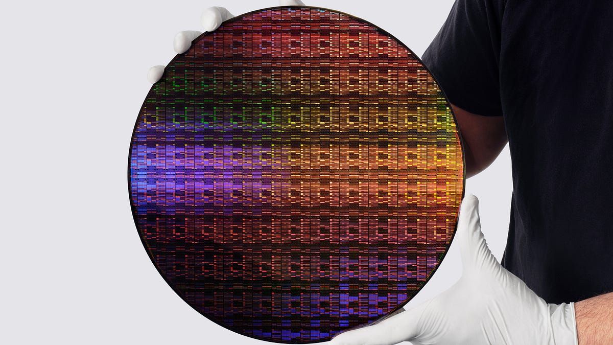
IBM's 0.7nm Node and NanoStack: A Technical Deep Dive into Next-Generation Semiconductor Technology
666 Million Transistors Per Square Millimeter
 morethanmoore.substack.com·22d ago
Comments
Sign in to join the conversation.
No comments yet. Be the first.