Understanding the Super Nintendo's Hardware Architecture: Clock Signals and Component Synchronization
Apr 1, 2024
Read the full articleYou might also wanna read

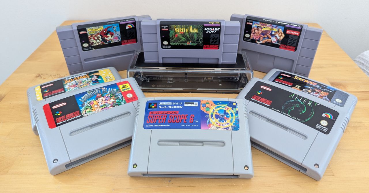
Epilogue SN Operator Review: A Premium FPGA Solution for Playing SNES Cartridges on Modern TVs
Provided you have a library of SNES cartridges, the SN Operator is a seamless plug-and-play system for easy ’90s nostalgia.
 wired.com·7d ago
SuperGuard: Comprehensive Testing for C++ Multi-Threading Primitives
Join Curtis Franklin, Editor in Chief of Circuit Cellar, and Marcel Beemster, CTO at Solid Sands, for a critical webinar, sponsored by Solid
 streamyard.com·13d ago
A Paper on Clock Distribution for Phase Coherent Operation of RTL-SDR Receivers
Modifying RTL-SDR dongles to run from the same clock source to create a phase-coherent receiver is something that has been done for many yea
rtl-sdr·4d ago
Comments
Sign in to join the conversation.
No comments yet. Be the first.