
























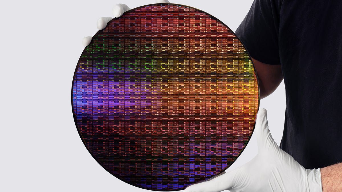
Intel Plans 14A2 Node With Dual Side Power To Battle TSMC And Samsung
The PowerVia back-side power delivery network (BSPDN) technology that Intel pioneered with its 18A fabrication process is brilliant, because separating power lines from data lines offers tremendous…
Read the full articleYou might also wanna read
TSMC A16 Backside Power at VLSI 2026
TSMC’s A16 technology , presented as Paper T1.5 at the June 2026 IEEE/JSAP VLSI Symposium , marks the company’s first angstrom-class CMOS pl


Researchers turn HBM on its side to tackle AI memory’s heat wall — Korean V-Die and Japanese MOSAIC designs promise higher bandwidth, denser stacks, and cooler future GPUs
Researchers in Korea and Japan have proposed sideways-stacked DRAM designs that could push future AI memory beyond conventional HBM limits b

Applied Materials VP discusses AI, energy demands, and semiconductor innovation beyond traditional scaling
In this interview, Sundeep Bajikar, Vice President of Corporate Strategy and Marketing at Applied Materials, discusses the evolving role of
 euractiv.com·9d ago
TSMC’s Photonic Ramp Could Be the Quiet Catalyst in AI Chips
Taiwan Semiconductor is quietly ramping a technology that could make today's AI chip bottlenecks look minor by comparison, and the window fo

Stacked-die half-bridge boosts MOSFET power density
Using a vertically stacked-die design, AOS's DFN6×5 AmpStack package integrates two MOSFETs configured as a high-side/low-side half-bridge.
IBM's 0.7nm Node and NanoStack: A Technical Deep Dive into Next-Generation Semiconductor Technology
666 Million Transistors Per Square Millimeter
 morethanmoore.substack.com·15d ago
Comments
Sign in to join the conversation.
No comments yet. Be the first.