Semiconductor Metrology Faces Challenges as Chip Manufacturing Goes Vertical
By
Pat Brans
Hand-rolled, kettle-boiled, baked to perfection. Worth every minute at the bakery.
Summary
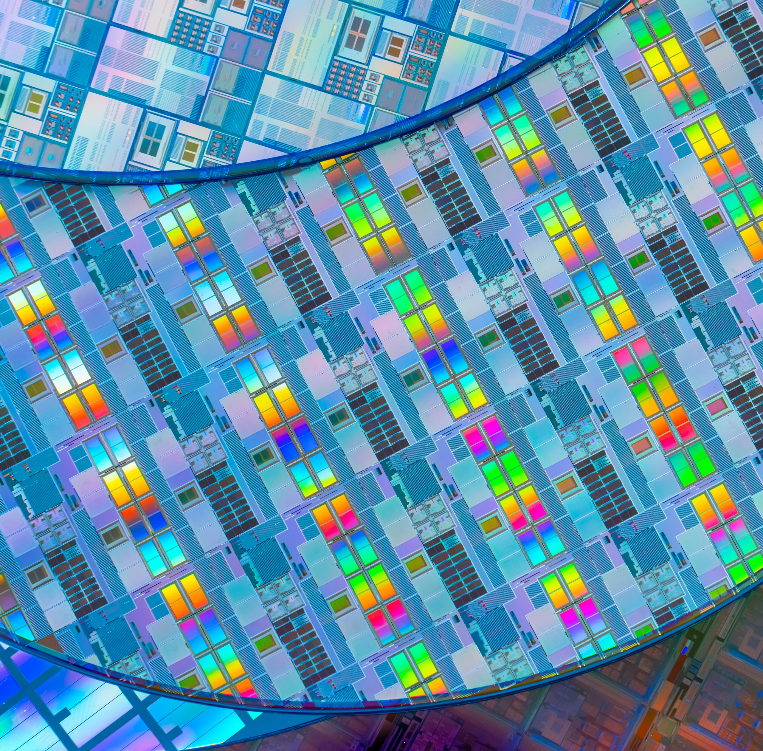
The semiconductor industry is facing a metrology crisis as chip manufacturing shifts from planar (2D) to vertical (3D) architectures. Traditional top-down inspection methods like optical metrology and CD-SEM, optimized for lateral scaling, are inadequate for measuring buried structures in gate-all-around transistors, HBM memory, vertically stacked NAND, and future CFET designs. The article explores how metrology tools must evolve to reconstruct and measure complex 3D structures deep within chips, highlighting the growing gap between advanced manufacturing capabilities and inspection technology.
Key quotes
· 3 pulledSemiconductor inspection has traditionally meant looking down.
Optical metrology and critical dimension scanning electron microscopy (CD-SEM) systems were optimized for lateral scaling, where the central challenge was shrinking dimensions across the surface of silicon.
Today, however, advanced-node manufacturing is moving increasingly into the Z-axis.
You might also wanna read


Industry Experts Discuss AI Applications in Semiconductor Chip Design
This article features a roundtable discussion with semiconductor industry experts from Cadence, Siemens EDA, Synopsys, Baya Systems, ChipAge
Bridging the Semiconductor Talent Gap: Cross-Training CS Students and AI-Assisted Hardware Design
The article discusses innovative approaches to address the talent shortage in the semiconductor industry, including cross-training computer

Managing 50 Million Pins: Automated Design Solutions for 3D IC and Chiplet Technology
The article discusses the semiconductor industry's shift to 3D IC technology and chiplets, highlighting the challenges of managing massive p
 allaboutcircuits.com·3mo ago
Texas Institute for Electronics Transforms 1980s Fab into World's Only 3D Heterogeneous Integration Facility for DARPA Program
The Texas Institute for Electronics (TIE) in Austin, Texas, is transforming a 1980s-era semiconductor fab into the world's only advanced pac
 spectrum.ieee.org·7mo ago
China Develops Prototype Semiconductor Manufacturing Machine Using Reverse-Engineered ASML Technology
Chinese scientists in Shenzhen have built a prototype machine capable of producing cutting-edge semiconductor chips for AI, smartphones, and
 japantimes.co.jp·5mo ago
Memory Manufacturers Shift Focus from Smartphones to Hyperscalers, Threatening 2026 Device Markets
The article analyzes a global memory shortage crisis driven by a fundamental shift in semiconductor manufacturing priorities. Rather than a
 idc.com·5mo ago